DEFECTS IN 2D MATERIALS
 Defects in materials are ubiquitous and at the nanoscale quantum effects, the impact is more pronounced, which could have a significant impact on device performance. At a high density of defect states, in a material with potential applications as a quantum transistor, intermediate band solar cells, etc. support the development of any practical applications, we need to develop a better understanding of the properties of disordered 2D materials and their hybrid structures. We use state-of-the-art techniques ranging from approaches in density functional theory to first-principles-based many-body model Hamiltonians to explore diverse arrays of materials.
INSULATORS & SEMICONDUCTORS
The electronic properties of a material play a critical role in material characterization and are crucial inputs in various computational approaches. Accurate determination of these properties is essential for the predictive capabilities of any computational model. For insulators and semiconductors (I&S), the predicted properties depend sensitively on the energy bandgap, which is the difference in energy between the highest occupied states (such as the HOMO in molecules) and the lowest unoccupied states (such as the LUMO in molecules). Obtaining an accurate and unambiguous determination of these states is vital for the successful implementation of I&S in actual device applications.
In our research group, we use state-of-the-art computational approaches to study a diverse range of materials for applications including, but not limited to, next-generation sensors and transistors, high-power devices, solar cells, photodetectors, and light emitters. Our goal is to achieve reliability and predictability in our computational models with a minimal number of parameters, ensuring the most accurate results for our clients.
HYBRID MATERIALS
Heterostructures, or the stacking of thin films made from at least two different materials, are the foundation of modern devices and technologies. The state-of-the-art heterostructure-based devices often involve stacks of crystals just a few nanometers thick, with the ultimate limit being a single-atomic-layer structure.
We are passionate about exploring and utilizing the potential of these low-dimensional hybrid structures in a variety of applications. Our research focuses on the development of heterostructures for thermoelectricity, photovoltaics and solar cells, hydrogen evolution using sunlight and semiconductors, and quantum transistors. We strive to push the limits of technology and bring innovative solutions to the market that will change the way we live and interact with our world.
NANOMATERIALS
At the nanoscale, materials exhibit exceptional electrical, optical, transport, and mechanical properties that are distinct from their macroscale counterparts. Our research focuses on the computational exploration of these unique properties to design electronic materials with new functionalities, such as efficient exciton transport and ultra-strong van der Waals forces.
We are particularly interested in two-dimensional materials (2DMs), which are materials that exist in the atomic limit, unlike bulk materials that have been reduced to the nanoscale. The discovery of graphene, a stable 2D monolayer of graphite, has led to the exploration of many other 2D materials with unique and novel properties. Our research aims to harness these properties for use in nanoelectronics and devices. By utilizing cutting-edge computational techniques, we are pushing the boundaries of materials science and engineering to create innovative solutions for real-world applications. Join us on our journey to discover the full potential of nanoscale materials.
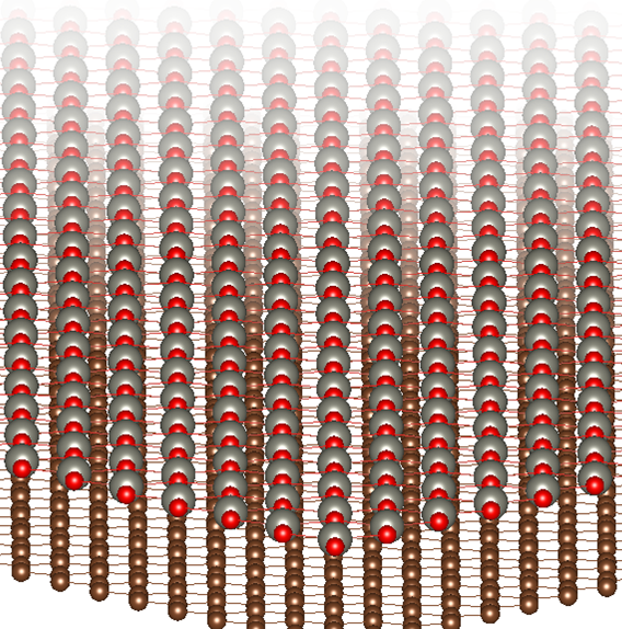
INTERCALATION IN LAYERED MATERIALS
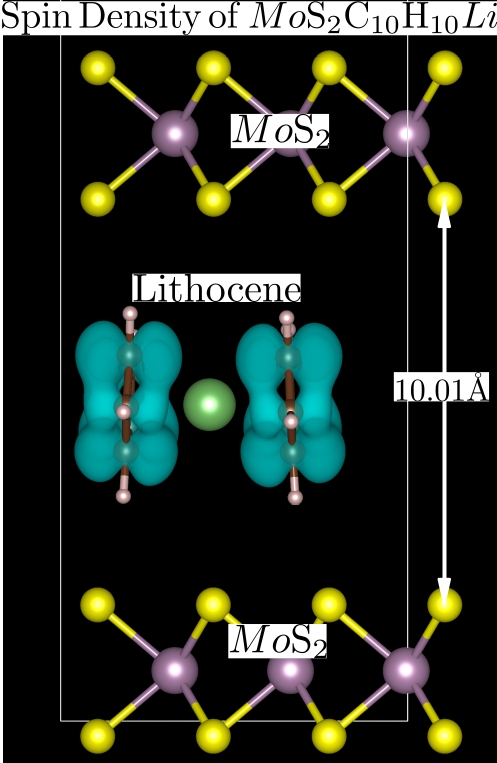
Chemical or electrical doping is a highly effective method for improving and controlling the carrier transport, density, and charge injection in materials. We specialize in intercalation as a means of achieving this goal. Intercalation involves inserting an intercalant, such as lithium, into layered transition metal dichalcogenides (TMDs) to improve their properties. We are exploring the use of various organometallic molecules, such as metallocene, to tune the properties of TMDs for use in battery applications and other systems.
Our first-principles calculations reveal that the electronic properties of vertically stacked 2D TMDs, such as HfS2, can be effectively tuned through intercalation. The intercalant behaves like a pseudo-alkali metal, transferring electrons to the host material and resulting in a shift of the Fermi level towards the empty states and an increase in current density. This process occurs through the transfer of charge from the intercalant to the host material, leading to doping in the vertically stacked van der Waals materials.
We are actively exploring other systems to uncover the full potential of intercalation as a means of improving and controlling the properties of materials. Join us in our quest to revolutionize materials science and engineering through innovative research and development.
EFFECTIVE MANY-BODY HAMILTONIAN FOR REAL MATERIALS
The description of real materials using dynamical mean-field approximation (DMFA)-based approaches needs realistic lattice and electronic structures, including interaction parameters. Since the dominant many-particle effects are local or short-range, the first-principles electronic structure needs to unto a basis set of local orbitals. via , which involves integrating out mainly the high-energy scales or focusing on the energy window of interest by constructing Wannier functions. as . In the electronic structure of a is mapped unto the Brillouin of the original cell to an effective disordered Hamiltonian. Sometimes, we are also interested in the effects of Coulomb interactions. There few ways to achieve this: 1) account for the effects of electron correlations via Hubbard interactions parameter; 2) self-consistently account for the many-body effects in the effective Hamiltonian by unfolding or a converged Green's function and screened Coulomb interactions (GW) calculations; and 3) construct an energy-dependent Anderson-Hubbard Hamiltonian. The last approach seems more natural and computationally efficient. It involves carrying out an independent GW calculation, e.g., self-consistent quasiparticle GW method for the parent material to a material-specific dynamical, screened electron-electron interaction.
ELECTRON LOCALIZATION
Since the pioneering work of P.W. Anderson in 1958 where he demonstrated that at large enough disorder, a conducting system could lose all its conductivity properties, i.e., become an insulator. A phenomenon that is now widely known as Anderson localization or metal-insulator transition. While Anderson's prediction remained unappreciated for more than a decade, it, however, has led to a new paradigm in the characterization of transport properties of disordered systems. The universality of Anderson localization has led to its application to other areas not limited to condensed matter systems, optical and ultracold atoms, disordered quantum systems, seismic analysis, photonic lattices in the form of matter waves, electromagnetic absorption in a disordered medium, superfluid helium in porous media, and even in molecular and biological systems.
To characterize localization, the most important quantity in the majority of physical or statistical problems is usually the “typical” value of the ‘random’ variable, which corresponds to the most probable value of the probability distribution function (PDF). It turns out that in most systems the nature of the PDF is a priori unknown since we have limited information via the moments or cumulants of the PDFs. Hence, the “typical” or the most probable value of the PDF is an essential quantity as it contains direct information of the system.
Unlike conventional continuous transition, the Anderson transition is a dynamical transition requiring a "proper" order parameter, which has remained a challenge in the mean-field treatment of Anderson localization. This is because different from some systems where the first moment (the arithmetic average) is a good estimate of the random variable, the Anderson localization is a non-self-averaging phenomenon. That is, close to the critical point if the system is phase coherent (mesoscopic regime), quantum interference effects cause the strong fluctuation of physical quantities such that the corresponding PDF of the local density of states is very asymmetric with long tails needing infinitely, many moments to describe it. In some cases, the corresponding moments might not even exist especially close to the critical point. Naturally, at the localization transitions, the typical local density of states vanishes while the continuous local spectrum becomes sets of delta-function peaks with long-lived resonance states. As a consequence, these long-lived resonance states at a given lattice site, acquire a finite escape rate which, according to the Fermi Golden rule, can be approximated as the inverse of the produce of the square of the hopping matrix and the local density of states in the neighborhood of a given lattice site.
Methods to better characterize the Anderson localization is still an area of active research. We recently developed the typical medium dynamical cluster approximation (TMDCA) that properly describes the Anderson localization transition predicting the critical quantities to within 2% of numerical exact approaches like the exact diagonalization, kernel polynomial method, and transfer-matrix-method. The TMDCA allows for resonance effects and by systematically increasing the system size, accounts for inter-site correlation effects, which are important for Anderson localization.
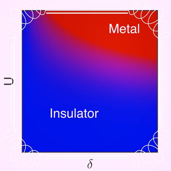
DEFECT-ENGINEERING
No material is truly "pure". For example, sample preparation or measurement one form of defects or the other could . We can as well intentionally introduce defects in the crystal lattice to improve on the device applications of the material. Such a large tunability of the electronic properties of materials via defect-engineering could aid in both fundamental understanding and discovery of new intermediate phases with novel functionalities. Often, materials are sensitive to external perturbations, e.g., magnetic field or doping and at the quantum mechanical level, these inhomogeneities appear to be intrinsic. We use various first-principles approaches to investigate how the presence of defects influences the behavior of materials. For example, defects can (a) turn metal into an insulator and . Such a transition, especially in 2D materials, could aid in the development of high electron mobility quantum transistors capable of operating in the terahertz regime (b) improve the chemical activity of layered materials like TiO2 or transition metal (c) induce novel magnetism in an otherwise non-magnetic dopant and semiconductor.
DATA-DRIVEN MACHINE-LEARNING-GUIDED MATERIALS DESIGN AND DISCOVERY

The screening of novel materials or the outright design of new materials with good performance and the modeling of the quantitative structure-property relationships are central to the interdisciplinary field of materials science. The combinatorial space of the potential chemical compositions is too large for an Edisonian approach that is both costly and time-consuming to be practical. Traditional experiments and computational modeling techniques often require a tremendous amount of time and resources; generally, severely limited by the experimental conditions and theoretical foundations. Therefore, it is imperative to develop a new method to accelerate the discovery and design approach for novel materials. Recently, new materials screening, design, and discovery using advances in materials informatics and machine learning have been receiving increasing attention. These advances have led to great improvements in both prediction accuracy and time efficiency.